How is PCB manufactured?
The process of PCB manufacturing can be complex which involves a lot of steps. The PCB can be single layer, double or multi-layer based on their usage and applications and depending on this there can be multiple steps that are involved in creating the PCBs. Skipping any one step can prove costly to the final electronic product but when done properly it can fulfill the needs in an electronic application.
What are the parts of PCB?
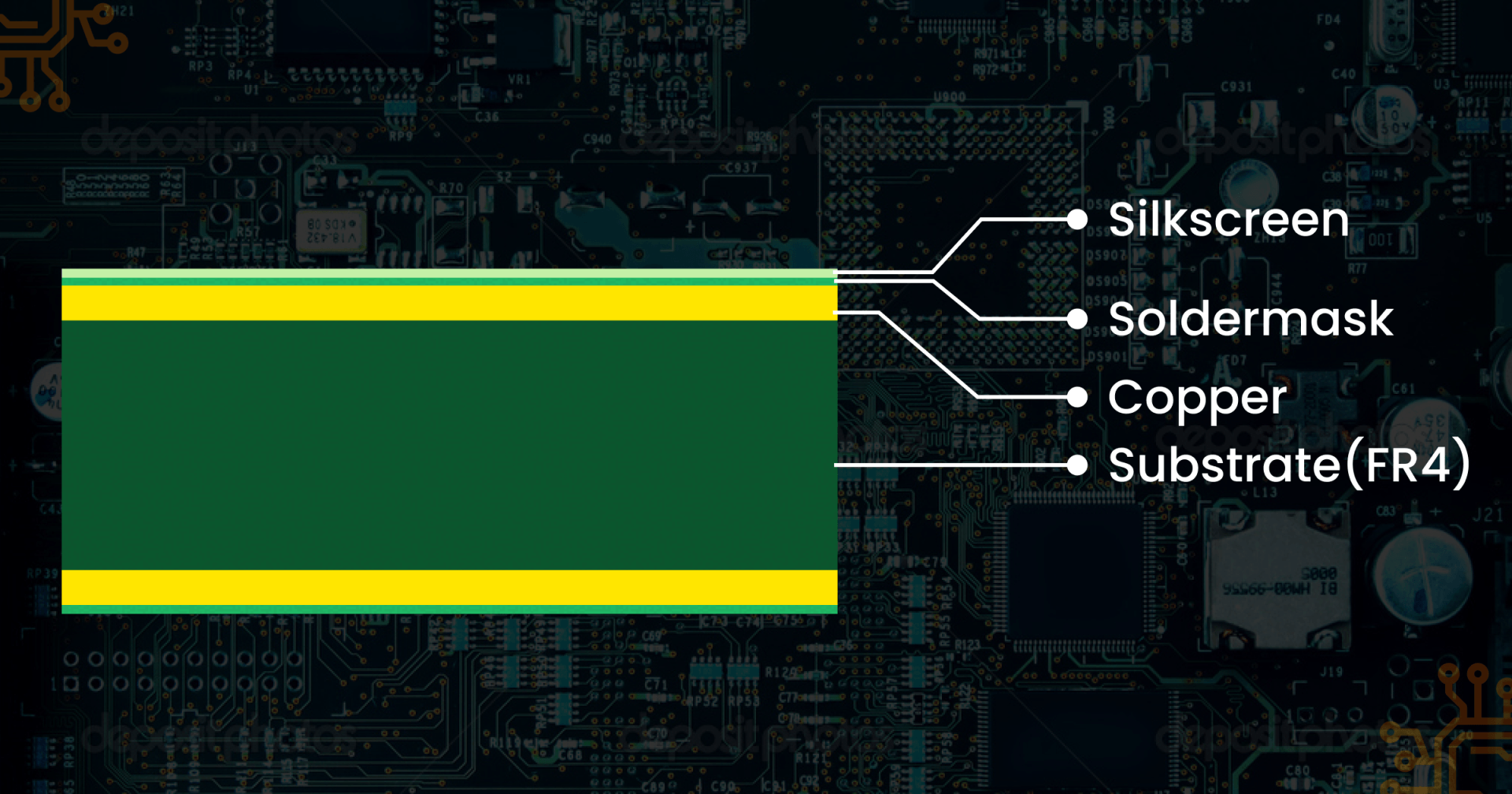
PCB has 4 main parts
Substrate: Substrate act as the skeleton in the final product. They are mainly made of high-quality fiberglass, that provides the strength to the PCB and prevents breakage.
Copper layer: Copper layer or coper foil can be used depending on the type of application and like metal, its primary use to carry electrical signals to and fro the PCB.
Solder Mask: Solder mask is a layer of polymer on the top of copper to prevent any short circuit that happens if the copper comes in contact with the outer environment.
Silkscreen: Silkscreen is given on the top of solder mask and is primarily for nomenclature details like number, logos, settings symbols, test points etc.
How is the PCB manufactured?
Now that we know the parts of PCB, its time to know more about the process of manufacturing the same. As told above, depending on the complexity and application the process steps differs and its mandatory to follow each and every step for the best results.
- Designing the PCB- Like ever good things begins with a plan, so does manufacturing the PCB. To design PCB respective software's are used. Extended Gerber — also known as IX274X is one of the commonly used software for designing PCB. Once the design blueprint is finalized its cross checked to make sure there are no errors. The final design is sent to fabrication office, where it's given a second check called design for manufacture check, where it checks the parameters design and tolerance is met the needed threshold.
- Design review and engineering- Checking the design for any flaws are error is the much-needed step to be done before jumpstarting the fabrication process and is done by an engineer who reports for any missing components or incorrect structures.
- Printing the PCB design- Like any other design, PCB designs need to be printed and a special kind of printer called plotter printer. The final product looks like a film that’s printed on the board itself.
The inside of the PCB uses
Black Ink-For copper traces and circuits of PCB
Clear Ink- For the nonconductive areas like fiberglass.
The outside
The outside of the PCB the color trend will be reversed.
Each PCB layer & accompanying solder mask will get its own film. After the film is printed the sheets are lined up and a hole called registration hole is punched through them, which is used as a guide to align the films later on.
- Printing the copper for inner layers- After the PCB is printed onto a piece of laminate material, a copper foil layer or copper coating layer. The copper is then prebonded to the same piece of laminate, the copper is etched then to reveal the blue print. Laminate is covered by photo sensitive material called resist which hardens when exposed to ultraviolet light and the resist helps to get a match between photos of blue print and what's to be printed to the photoresist.
Once the resist and laminate are lined up using the registration hole they receive a blast of UV light, the light passes through the translucent material which helps to harden the photoresist. The black ink doesn’t prevent the light from getting into areas that shouldn’t be hardened.
After the board has been prepared its washed with alkaline solution to remove any photoresists and the board is pressure washed to remove anything left on the surface of the board and left to dry. After drying the only resist should be on the top of copper. Finally, the technical looks over the PCB for any flaws or errors.
- Etch the inner layers to remove the copper- Inner layer of the board need to have the extra layer to be removed. Etching covers the needed copper exposing the rest to a chemical and hence removing it. The amount of solvent used depends on the amount of copper used as for large applications the copper used will be more.
- Layer alignment- After each layer of the PCB has been cleaned its ready for alignment and optical inspection. The holes are used to align the sheets together. To align the layers, a technician places in a special type of punching material called optical punch. Optical punch drives a pin through the holes to line up the layers of PCB.
- Automated optical inspection- Once the step 6 is completed the optical inspection is carried out so that there are no errors being there. On the completion of optical inspection an AOI machine inspection is carried out to check for any short circuits, extra copper which should be removed before further.
- Laminating the PCB layer- Once the the inspection is done, the layers should be fused and the lamination is done in basically two steps- the laying step and lamination step.
Once the outer and inner layers are ready, they should be sandwiched together to get the final picture. For this a special type of table is used on which each layer is secured with a pin and special metal clamps are used. A layer of pre-impregnated epoxy resin is placed followed by a layer of substrate then a copper foil layer. The copper layer is followed by many layers of pre-impregnated resin, finished off with a copper plate called press plate.
Pins are pressed through the sheet to ensure that the layers stay intact. After the copper plate is placed next step is to the stack to be pressed which is done using a mechanical press. The stack is then taken to the laminating press where heat and pressure is applied to the stack. Heat causes the resin to melt and pressure applied causes the layers to press and fuse together. After the layers are pressed together the top press plates & pins are removed.
- Drilling- Holes are drilled using the extended Gerber design as the reference and is done using computer guided drill. X ray machine is used to drill the holes, then the registration holes are drilled so that PCB stack layers can be secured.
10. PCB plating- Plating uses different types of chemicals to fuse the layers together. The process called as bathing is carried out where the PCB layers are bathed in a series of chemicals. In bathing process, the panel is coated with a micron thick layer of copper.
11. Outer Layer Imaging- In step 4, a photo resist was applied to the PCB panel, similarly here also a photoresist coating needs to be applied. But this time only the outer layer needs to be coated as they are the ones to be imaged and plating is done using tin to secure the copper of outside layer.
12.Outer layer etching- The outer tin covering act as a covering for the copper layer from etching. Any unwanted copper is removed using the solvent as before. Previously for inner layer etching dark ink is used for conductive areas and light ink for non-conductive areas, these ink are reversed for outer layers. The non-conductive area has dark ink and conductive area has light ink. The light ink allows the tin plating to cover and protect the copper.
13. Outer layer AOI- As done with the inner layer, the outer layer too must go through the set of inspections. Any unwanted coating is checked along with the design specifications. It will only go through the next steps if all the conditions needed to perfect the design are met.
14. Solder mask application- Once the panel is clean, they will now go through solder mask application. Each panel has epoxy resin and solder mask fil covering. UV light is used to check where the solder mask need to be removed. Once the unwanted solder mask is removed, its taken to an oven to cure the mask, this mask provides extra protection for the copper from corrosion and oxidation.
15.Silk screen application- All the vital data should be written on the board itself for better convenience and is also called legend printing. The data to be given include
- Manufacturer data & logo
- Company ID & Specifications
- Warnings
- Pin locators & similar identifications.
- Part numbers
Using an inkjet printer the information is printed on the board and is proceeded for further steps.
16.Finishing the PCB- Finishing requires to be done using conductive material like below ones
- Electroless nickel electroless palladium immersion gold- High solder strength, prevents corrosion, require proper maintenance & less cost effective.
- Organic Solderability Preservative- Cost effective, short shelf life, RoHS complaint.
- Immersion tin- RoHS compliant, tight tolerance on holes, useful for press fit applications.
- Lead free HASL- Long lasting, reworkable, contains lead, not RoHS compliant, cost effective.
- Electroless nickel immersion gold- Expensive, RoHS compliant, long shelf life.
- Hard Gold- Long shelf life, durable, lead free, expensive.
- Immersion silver- lead free, the finish can oxidise and tarnish, low signal.
17. Electrical reliability test- Once the coating and curing is done, different electrical tests are conducted to check the reliability. Electrical testing should adhere to standards of IPC-9252. One test is circuit continuity test and other one is isolation test. The continuity test checks for any circuit disconnections. The isolation test checks for isolation values of PCB parts to check for any shorts.
18.Profiling & route out- profiling will identify shape & size of the PCBs. Routing out or scoring allows the easier separation of boards. A router or CNC machine creates several small pieces along the edge of the board so that it can quickly break off without damage.
19.Quality check and inspection- PCB again undergoes final inspection. It checks for whether the hole size are matching for all layers, the board have its specific dimensions, clean and dust free, not having sharp edges.
20.Packaging & Delivery- Packaging involves material that seals the board from dust and foreign particles. The sealed boards are then put in containers that protect them damage from shipping.
PCB manufacturing is no piece of cake, it involves a lot of articulate steps that need to be followed. We design our processes to accommodate all type of printed circuit board assembly, whether they are thin, thick, or flexible, small or large, single sided or double sided, single layered or multi-layered or even mixed technology. With our connections to the large PCB manufacturers in the Far East we can provide you with PCB assemblies that use the best quality PCB’s at the lowest cost New Paragraph